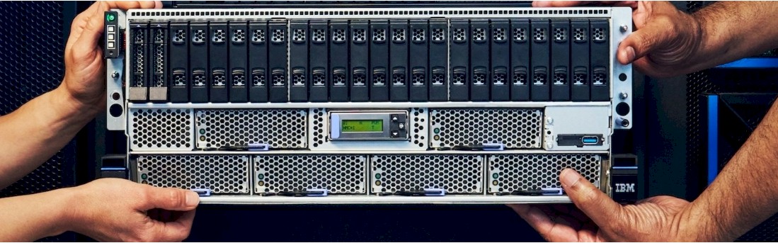
If you need a big, badass box that can support tens of terabytes of memory, dozens of PCI-Express peripheral slots, thousands of directly attached storage devices, all feeding into hundreds of cores that can span that memory footprint with lots of bandwidth, you do not have a lot of options.
This is one reason why IBM still has a Power Systems server business based on its Power family of RISC processors, which support IBM’s homegrown variant of Unix, its proprietary and venerable IBM i (formerly OS/400), and Linux as their operating systems. And the profitability of that big iron and the utter dependence that customers who need big NUMA machines have on these boxes to support massive transactional database management systems and the applications that wrap around them, is why Big Blue can still afford to invest in its Power processors.
Hence, the launch of the Power11 processor last week, which will ship across a range of entry, midrange, and enterprise servers starting on July 25.
The Power11 chip is, in a way, a deep bin sort of the Power10 chip that first debuted in September 2021.
The Power10 chip had been through the wringer, with canceled 10 nanometer and then 7 nanometer manufacturing processes from chip foundry partner GlobalFoundries. These same process transitions were an epic fail at Intel as well, and delay after delay in manufacturing gave AMD the change to leapfrog the Xeon X86 server chips with its compatible Epycs and AMD has been gaining share since.
GlobalFoundries took over IBM Microelectronics in October 2014 and assumed the productization of Big Blue’s 14 nanometer process that was, er, in process at the time. As best as we can figure, the Power9 chip that was etched in 14 nanometers by GlobalFoundries was about a year late to market, and it took IBM a full year to ramp up its production in 2018. (The initial Power9 delivered in late 2017 went into the “Summit” supercomputer at Oak Ridge National Laboratory and into the “Sierra” supercomputer at Lawrence Livermore National Laboratory and were paired over NVLink interconnects to share memory with Nvidia “Volta” V100 GPU accelerators. There was supposed to be a Power9’ – that is a “prime” sign, meant to designate something less than a “+” update that usually meant a process shrink and often a doubling up of chips in a socket in the Power processor line – but it never happened. (The Power8’ was a testbed for tightly coupling Power8 chips with NVLink ports to Nvidia “Pascal” P100 GPU accelerators.)
The original Power10 plan, as we discussed back in June 2021 when IBM sued GlobalFoundries for breach of contract, was to move to 10 nanometer processes and a new Power microarchitecture, doubling up the core counts from Power9. That would have meant 24 cores with eight threads per core (what IBM calls SMT8) or 48 cores with four threads per core (what it calls SMT4). This chip was due in 2020, with faster OpenCAPI and NVLink direct I/O and memory sharing ports. A follow-on Power11 was slated for several years after that, presumably with a 7 nanometer process and definitely with much wider vector processing engines in its cores.
Somewhere along the way, GlobalFoundries told IBM it was going to skip to 7 nanometers because of the 10 nanometer delays, and IBM got to reworking the Power10 design. At the 7 nanometer node, the IBM roadmaps that we have seen suggest that Big Blue would deliver Power10 in variants of with 60 SMT4 cores and 30 SMT8 cores, for a total of 240 threads either way, using the GlobalFoundries 7 nanometer process. In August 2018, GlobalFoundries spiked its dual-prong effort to create 7 nanometer processes (one using standard immersion lithography and the other using more expensive extreme ultraviolet (EUV) techniques, leaving Big Blue in the lurch for a foundry for its Power and System z mainframe CPUs.
IBM went to Samsung, which makes its own smartphone chips and which very much wanted to create high performance processes at 7 nanometer and smaller nodes for larger compute engines. IBM was a perfect initial customer from which to learn the process, since it had decades of expertise in developing chips and making them.
As part of that move to Samsung, IBM set about to revamp the Power instruction set and architecture, and added matrix math units to the integer cores and floating point vectors already in the Power design. This revamp, we think, would have come with a Power11 generation had all of the manufacturing issues not delayed Power10 and then Power11. The coronavirus pandemic also gave IBM cover to take its time on Power10 and do it right. In this sense, the Power10 as delivered is what we think Power11 might have been. So Power10 was really Power11 and Power11 is really Power11+, if you want to think of it abstractly.
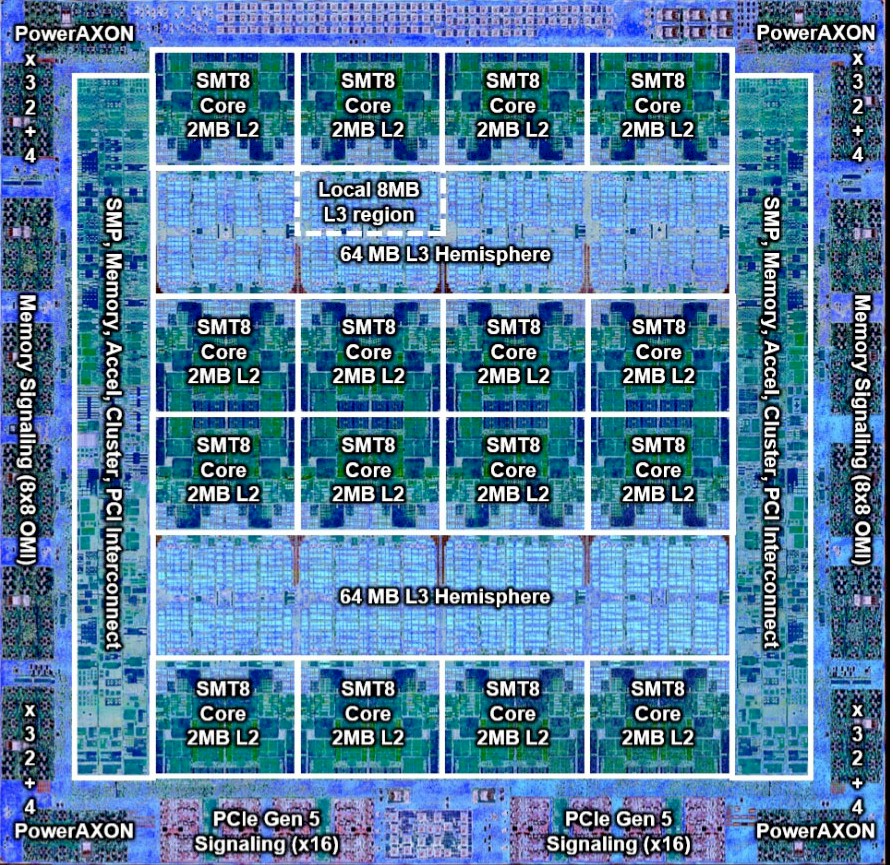
The Power10 and Power11 chips as delivered both have sixteen cores with the same 18 billion transistors; the difference is how the cores are used and their clock speeds. The Power10 chips had the same 128 MB of L3 cache etched on them in two banks, with the SMT8 cores wrapped around them with 2 MB of L2 cache each. The big difference is that with Power11, all sixteen of the cores can be activated to run an operating system, whereas with Power10 a maximum of fifteen cores were available for use because with the initial 7 nanometer Samsung process, at least one of the cores was going to be a dud. And based on the SKUs for Power10, it looks like quite a few more were duds. (This is true of Intel and AMD X86 server processors, too, which is how the SKU stacks scale down to a small number of cores.)
With Power11, for the so-called “scale out” systems with one or two sockets, IBM has Power11 chips with four, eight, ten, twelve, or fifteen usable cores and makes use of these with single chip modules (what it calls SCMs) and dual chip modules (which are called DCMs). Frequencies range from 2.4 GHz to 4.15 GHz in the DCMs to 3 GHz to 4.2 GHz in the SCMs. There is a special variant of the DCM where the second chip in the socket has all of its cores deactivated (either intentionally or through bad yield) but all of the I/O capabilities of the chip are available. So this entry SCM, or eSCM as IBM calls it, has four or ten active cores on one die and none on the second, but twice as much I/O as you would expect.
In some of the documentation that we have seen, there are tables that say the Power11 chip has 30 billion transistors and a clock speed that ranges from 3.8 GHz to 4.4 GHz, and a die size of 654 mm2 compared to a die size of 602 mm2 and clock speeds of between 3.75 GHz and 4.15 GHz for Power10. We have no idea where this higher transistor count and die area is coming from in these tables, and have reached out to IBM for clarification. As far as we know, the die size and transistor count of the Power10 and Power11 dies are the same; how many of these transistors were usable has certainly changed.
On the big, bad Power E1180 server, the machine is nearly identical to the Power E1080 that shipped back in 2021. One big difference is that DDR5 memory comes in the Power E1180 by default and this was an upgrade option at the tail end of the Power E1080 generation, which started out with DDR4 memory. Customers who bought E1080s and spent a fortune on DDR4 memory are allowed to upgrade their processors to Power11 but keep the DDR4 memory in the box, saving them a fortune by sacrificing some performance specs in the bargain. IBM can do this because it has a differential interface to its memory through the OpenCAPI Memory Interface, or OMI, with the DDR4 or DDR5 protocol being implemented on the memory chips instead of the controllers on the Power10 or Power11 chips.
This is a smart way to do main memory, and the industry could learn a thing or two from what IBM has done with OMI memory on Power Systems.
Here is what the Power11 chip looks like, and it should look familiar to you as the Power10 as well:
And here is a block diagram that shows the lanes coming off the Power11 SCM, which is the same as the Power10 SCM with some packaging tweaks to improve energy efficiency:
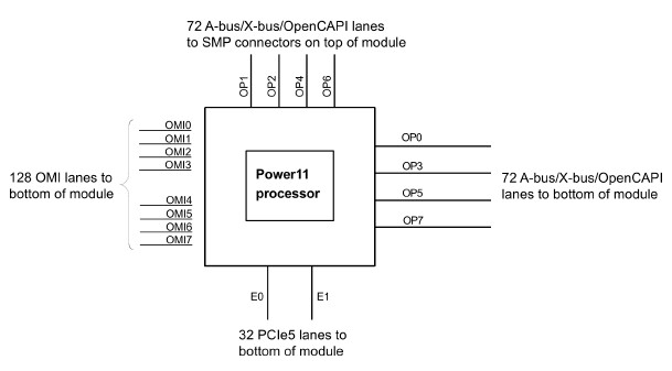
The Power11 chip has 72 I/O lanes coming out of the top of the SCM module that can support X-bus interconnects between CPU sockets within a single node as well as A-bus NUMA links across multiple nodes. It is not clear what the X bus links are running at in Power11, but we suspect it is 50 Gb/sec; we know the A-bus links run at 32 Gb/sec.
With four sockets per node and four nodes in a single shared memory system, the Power E1180 can deliver a maximum of 256 cores running at 4.4 GHz, with up to 64 TB of main memory. Given the cost of memory, we expect for big Power E1180 machines in the real world – even those running SAP HANA in-memory databases and their applications – will top out at 16 TB, and maybe once in a while at 32 TB. Memory is just to damned expensive to splurged on it unless you really have a business case.
This is a very big box, and one that has I/O and memory balanced well against compute. AMD systems top out at two CPUs in a NUMA cluster, with 128 cores and 256 threads running at 2.7 GHz with the plain vanilla “Turin” Epyc 9005s with the Zen 5 cores, and 128 cores and 256 threads running at 2.25 GHz with the “Turin” Zen 5c variants that double up the cores by cutting the L3 cache size used on the die in half. Now, granted, that machine running full-bore 6.4 GHz DDR5 memory can deliver 1.5 TB/sec of memory bandwidth. With 64 GB DDR5 DIMMs, which we think is a practical upper limit because of price, this machine would have 3 TB of memory.
IBM slows the DDR5 memory way down and puts sixteen memory controllers on the Power11 die so the memory runs cooler and more reliably to get 12.8 TB/sec of memory out of a sixteen-way Power11 server and to also get 16 TB of memory across sixteen sockets using 64 GB differential DIMMs. (It has 32 GB, 64 GB, 128 GB, and 256 GB D-DIMMs available.)
An eight-way server using Intel “Granite Rapids” Xeon 6 processors would top out at 86 cores per socket, or 688 cores across the NUMA machine, but these run at a mere 2 GHz. That Intel Xeon 6 system with 64 GB DDR5 DIMMs running at 6.4 GHz would deliver 8 TB of capacity and 5.5 TB of bandwidth across all of the memory controllers in the machine.
IBM has been blurring the lines between memory and I/O and accelerators for many years, and we showed off some interesting options way back in August 2018 that IBM could do with Power9 processors. It is easy to dial back the cores relative to memory bandwidth in a Power server – just buy processor modules that have a lot of dud cores on them. You can dial up the memory capacity of the system based on the capacity of the DIMMs. The bandwidth is what it is. You can dial that up by filling memory slots or down by not filling them.
But it is hard to push up the core count if you need more compute relative to the memory capacity or the memory bandwidth. Thus, we suggest that IBM create something called an extended DCM, or an xDCM, that converts some of the OMI memory ports and OpenCAPI ports on the system to X-bus and A-bus NUMA links, boosting the scalability of the top-end Power11 machine by scaling up the Power E1180 node above four-way NUMA or the system by adding more NUMA nodes to the box. We suspect that the latter might work better.
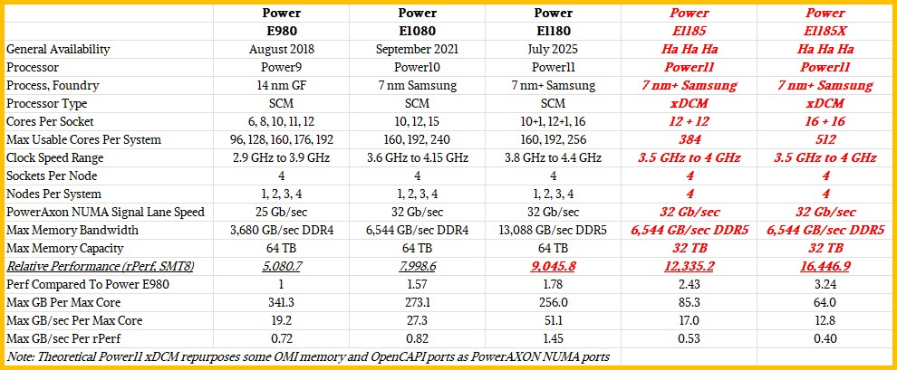
In any event, here is how the last three generations of top-end Power Systems machines based on Power9, Power10, and Power11 processors stack up, and how the theoretical Power E1185 and Power E1185X might compare:
We have no idea how expensive such a tweak might be, but adding more cores means that IBM can add more virtual machines to the box, helping with consolidation of enterprise workloads onto a big box.
